Lab 1:FPGA and MCU Setup and Testing
Introduction
In this lab, an FPGA and MCU were assembled on a board and tested to ensure functionality. First, all of the components were souldered onto the board. Then the FPGA was used to take input from the 4 input DIP switch and power 3 on-board LEDs and a seven segment display. The FPGA powered one of the LEDs to blink at 2.4 Hz, one to perform an exclusive or of the first two switch inputs, and one to perform an and of the second two switch inputs. The FPGA also performed logic to display the corresponding hexadecimal digit to the input from the four switches.
Design and Testing Methodology
The task of blinking an LED at 2.4 Hz was completed by making use of the on-board high-speed oscillator (HSOSC) from te iCE40 UltraPlus primative library. This library was used to make a signal that oscillated at 48 MHz. A counter that counted to 10,000,000 was then used to generate a signal that oscillated at 2.4 Hz. This signal was then used to drive one on-board LED. The second two LEDs were driven by combinational logic done on the FPGA. This was completed using simple assign statements. The seven segment display was driven by a module that took the inputs from the 4 switches and did the combinational logic to drive the pins of the seven segment display. This was completed using a case statement. The seven segment display used was a common annode one, which meant that power was driven to it through a common anode and then the display was controlled by driving the corresponding cathode pins of the seven segment display to 0. These pins were connected to the FPGA and a current limiting resistor. This was tested with a simulation of the systemverilog in ModelSim. A testbench module was created to instanstiate an instance the logic design for the FPGA, and then apply test vectors to ensure that the design functions as expected. Within the repository the sim folder contains the systemverilog test bench. Because of how the timing in the simulation works, it is not reasonable to test the LED blinking at 2.4 Hz in simulation. Thus, the blinking LED was tested using an oscilloscope to measure the frequency of the LED signal.
Technical Documentation:
The sourcecode for the project can be found in the Github repository.
Figure 1: Block Diagram
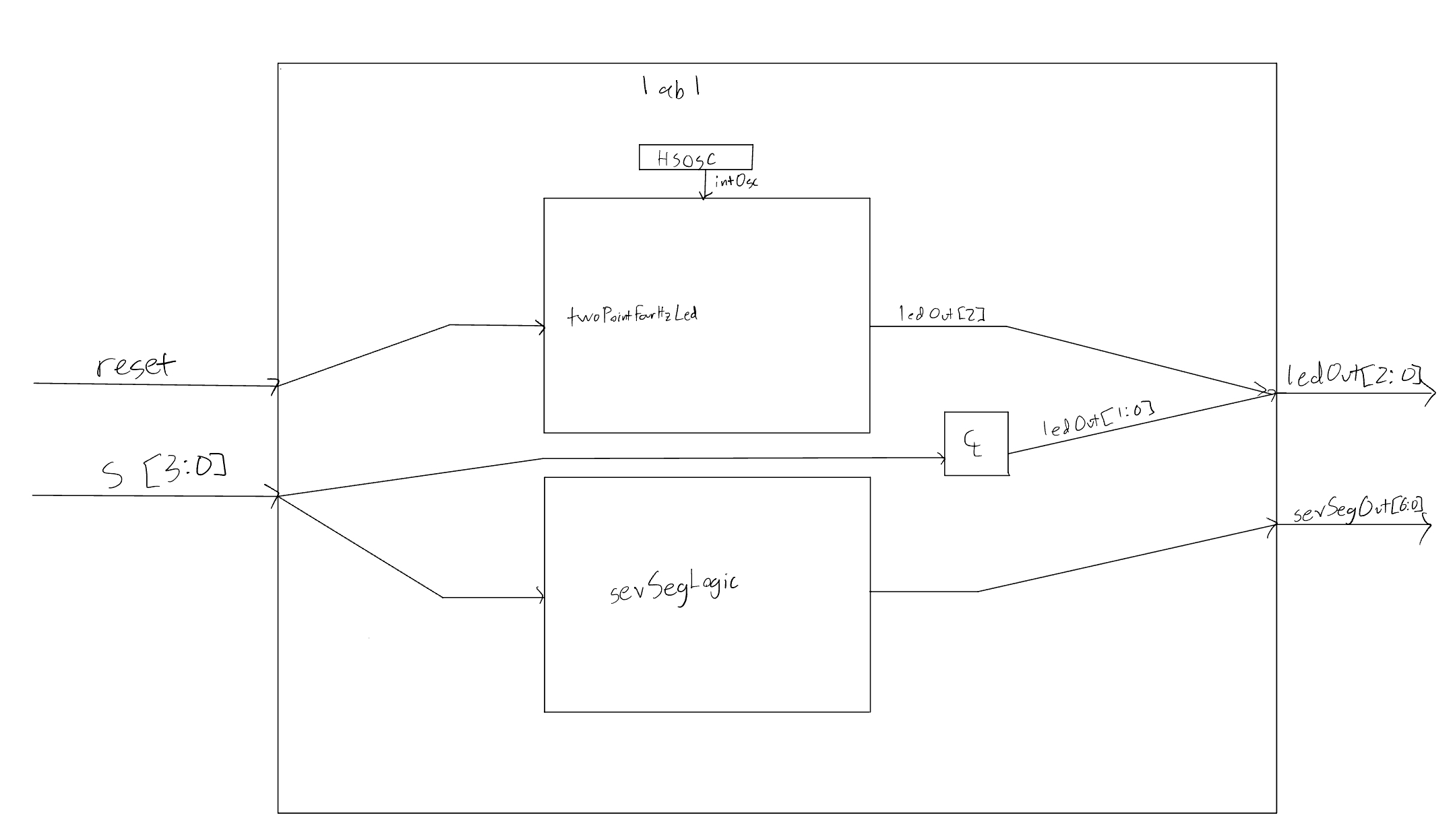 Figure 1 showcases the design implimented on the FPGA, with the lab1 module containing the oscillator and seven segment display logic modules.
Figure 2: Schematic
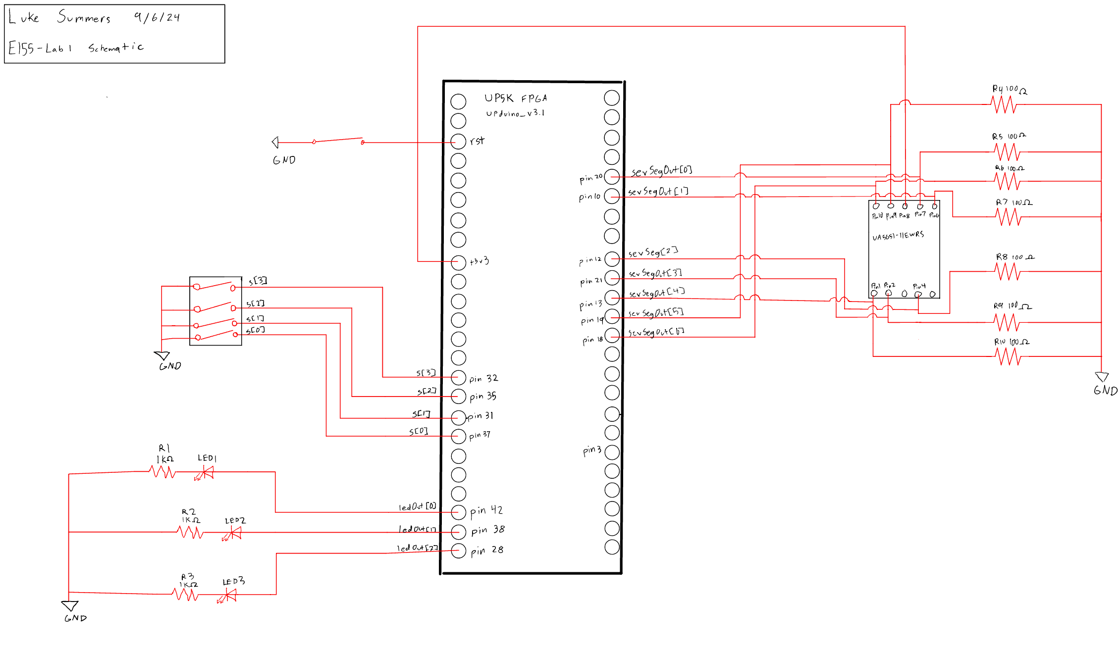 Figure 2 shows the circuit for the lab. The LEDs were connected to current limiting resistors of 1k \(\Omega\) for the on-board LEDs and 100 \(\Omega\) for the seven segment display LEDs to ensure the circuit did not draw too much current from the FPGA pins. The resistor values for the seven segment display were found by solving for R in V = IR with the voltage and desired current of the circuit. The voltage drop of the LED was 1.5, and the desired current was 5-20 mA. Solving for R with 5 and 20 mA, we see that the desired resistor is between 75 and 300 \(\Omega\).
Results and Discussion
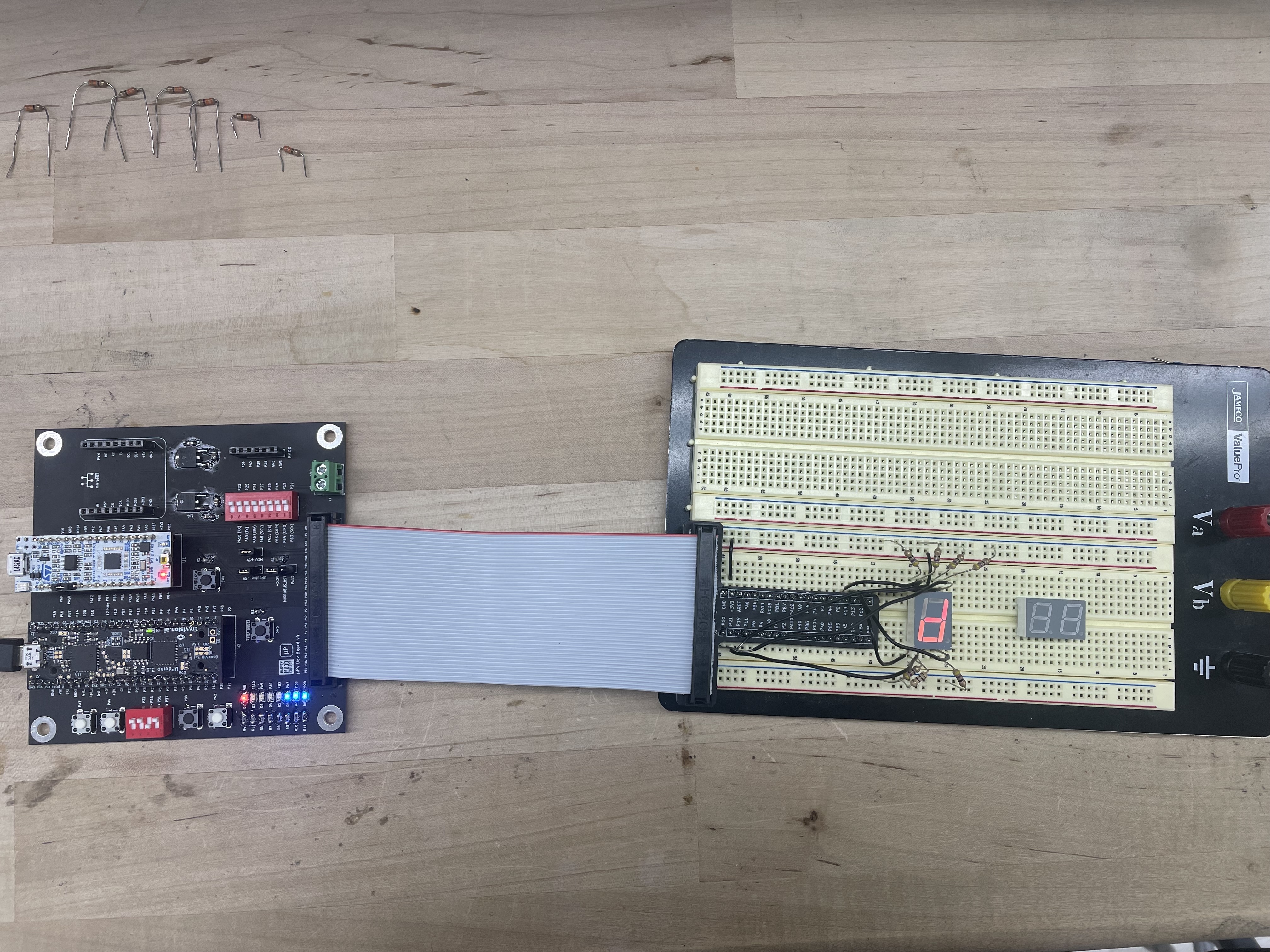 The design was succesful both in similation and in reality. The systemverilog design passed the test bench as the output signals match the expected output signals and the test bench module ran succesfully with no errors. Moving the design into a circuit, the circuit seen in Figure 2 was succesful in producing the desired LED signals. This was seen through an oscilloscope reading and observation of the other LEDs.
Figure 3: Oscilloscope Reading
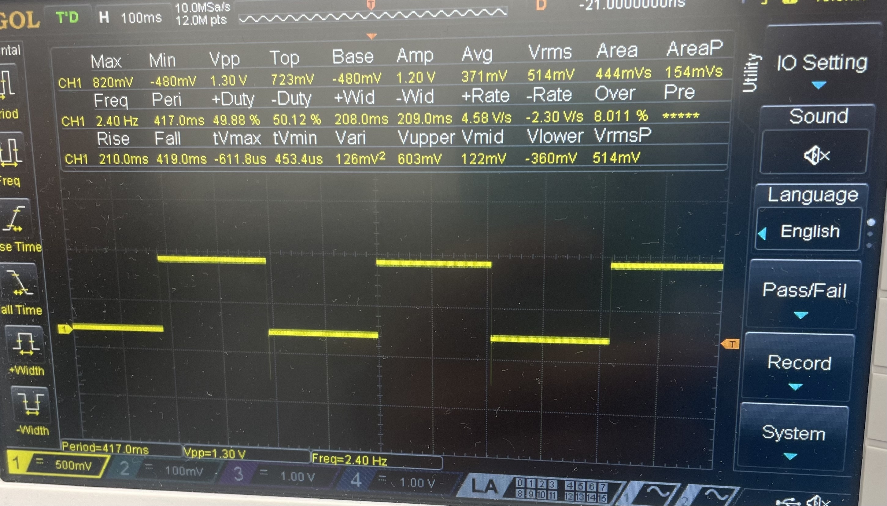 Figure 3 shows a picture taken of an oscilloscope reading of the signal blinking at 2.4 Hz for one of the on-board LEDs.
Figure 4: Testbench Simulation
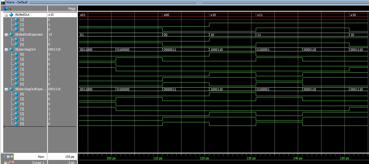 Figure 4 shows a screenshot of the waves produced by the test bench simulation.
Figure 5: Example of on Board LEDs
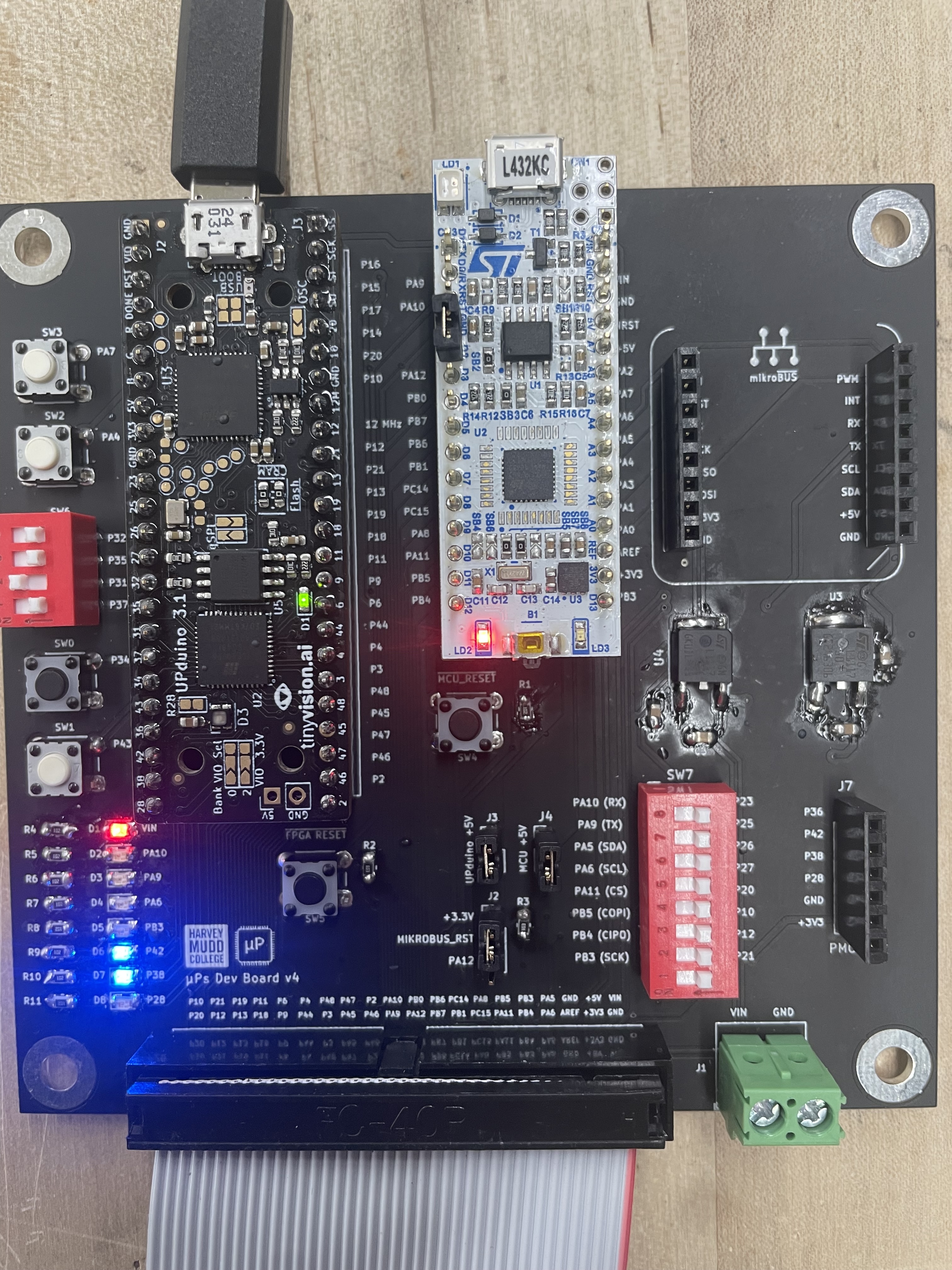 Figure 5 shows a picture of the board with the input switches set to an inbut of ‘1101’. Since the exclusive or of the 2 least significant bits and the and of the 2 most significant bits are both true, both LEDs are lit. The third LED was caught at a point of being not lit.
Figure 6: Example of Seven Segment Display
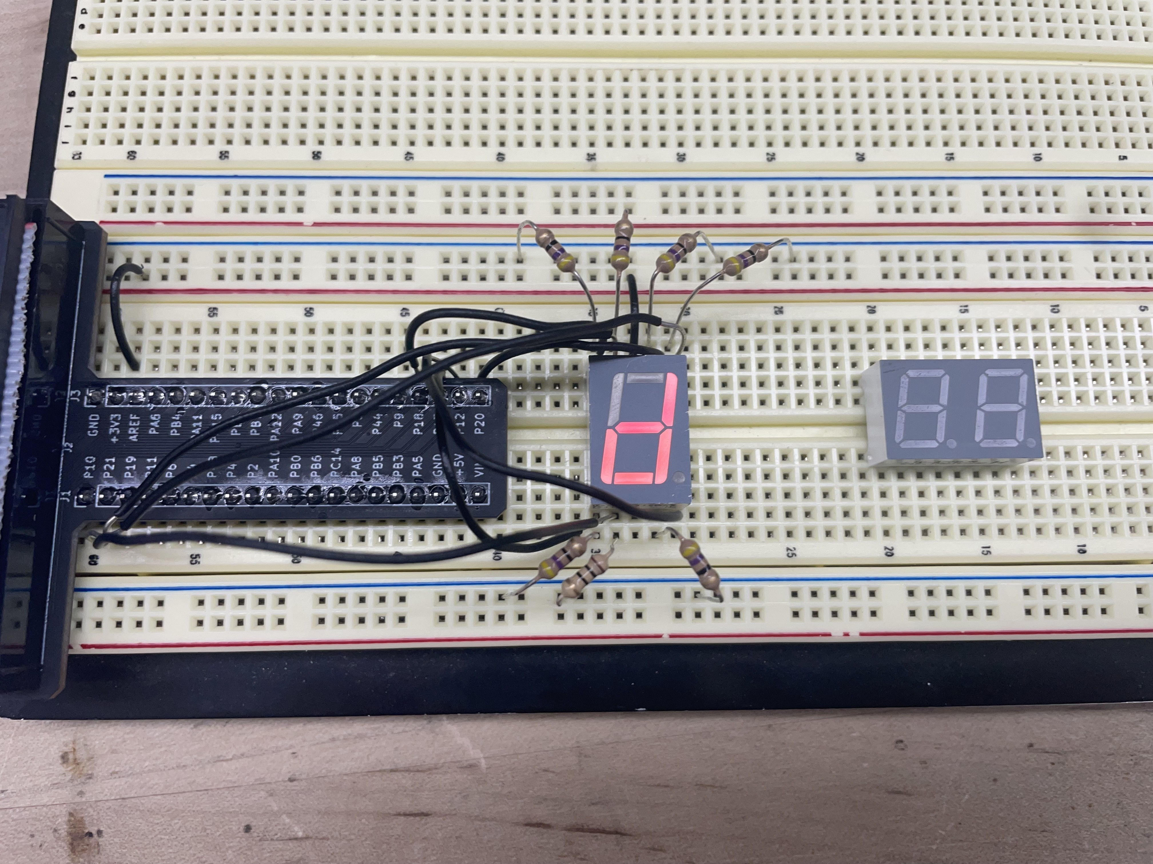 Figure 6 shows the seven segment display on the same input as seen in the previous figure. ‘1101’ corresponds to ‘d’ in hexadecimal, and the representation for ‘d’ chosen is shown in the figure on the seven segment display.
Conclusion
The design performed the desired logic in simulation and in a circuit. This proved all the components of the circuit board assembled to be functioning. I spent a total of 18 hours on this lab.