Lab 3: Keypad Scanner
Introduction
In this lab the FPGA was used to take input from a 4 \(\times\) 4 keypad and then displayed the 2 most recently pressed digits on a dual seven segment display. Recieving the input from the keypad was done using a finite state machine, and then the display was drivin with the same modules used in Lab 2. Thus the main task of the lab was designing the FSM to correctly read inputs from the keypad scanner.
Design and Testing Methodology
The task was completed using a finite state machine and a decoder to decode the output signals from the FSM. The onboard high speed oscillator was used to produce the clock signal to drive the other modules. A synchronizer module was used to synchronize the inputs from the keypad columns for the FSM. The finite state machine that read the input from the keypad scanner would continuously power one row of the scanner at a time until a button was pressed, connecting a row to a column and powering one of the column bits. The design implimented would register one key press if a key was held, and it would ignore any other keys pressed while a key was held. In order to ignore switch bouncing, the FSM design had two hold states for the signal to bounce whenever a button was pressed. This meant that the system had to be clocked at a frequency slow enough to where 2 cycles would be enough to handle the switch bouncing. A more complex design could have been used to handle switch bouncing at a faster clock frequency but that was not necessary for this lab. When a key was pressed, it would set the enable signal for the FSM decoder to then update the input signals to the display. The FSM decoder completed the logic to decode the row and column into the digit pressed, and then used an enabled flip flop to update the two output digit signals. The task of driving the two displays was done by using a module to multiplex the switch inputs and then feed this signal into the seven segment display decoder module. The input multiplexer module would on every positive edge of the clock switch between outputing each switch signal. This output signal was then inputed into a module that decoded the signal into the corresponding signal to drive the LEDs of the display. Two enable signals were also output for transistors used to drive the displays. A testbench was created for the FSM, decoder, and lab3 top modules in order to test their functionality in simulation. The circuit for the design included the dual seven segment display, two PNP transistors for driving the display, and the keypad scanner. The seven segment displays would draw too much current from the FPGA pin, so a transistor was used to help supply current. Two PNP transistors were used, which were switched on and off by the enable signals to drive displaying either digit. Since the pins connected to the keypad would be floating when a button was not pressed, pull down resistors were used on these signals.
Technical Documentation:
The sourcecode for the project can be found in the Github repository.
Block Diagram

Figure 1 shows the design implimented on the FPGA.
Schematic
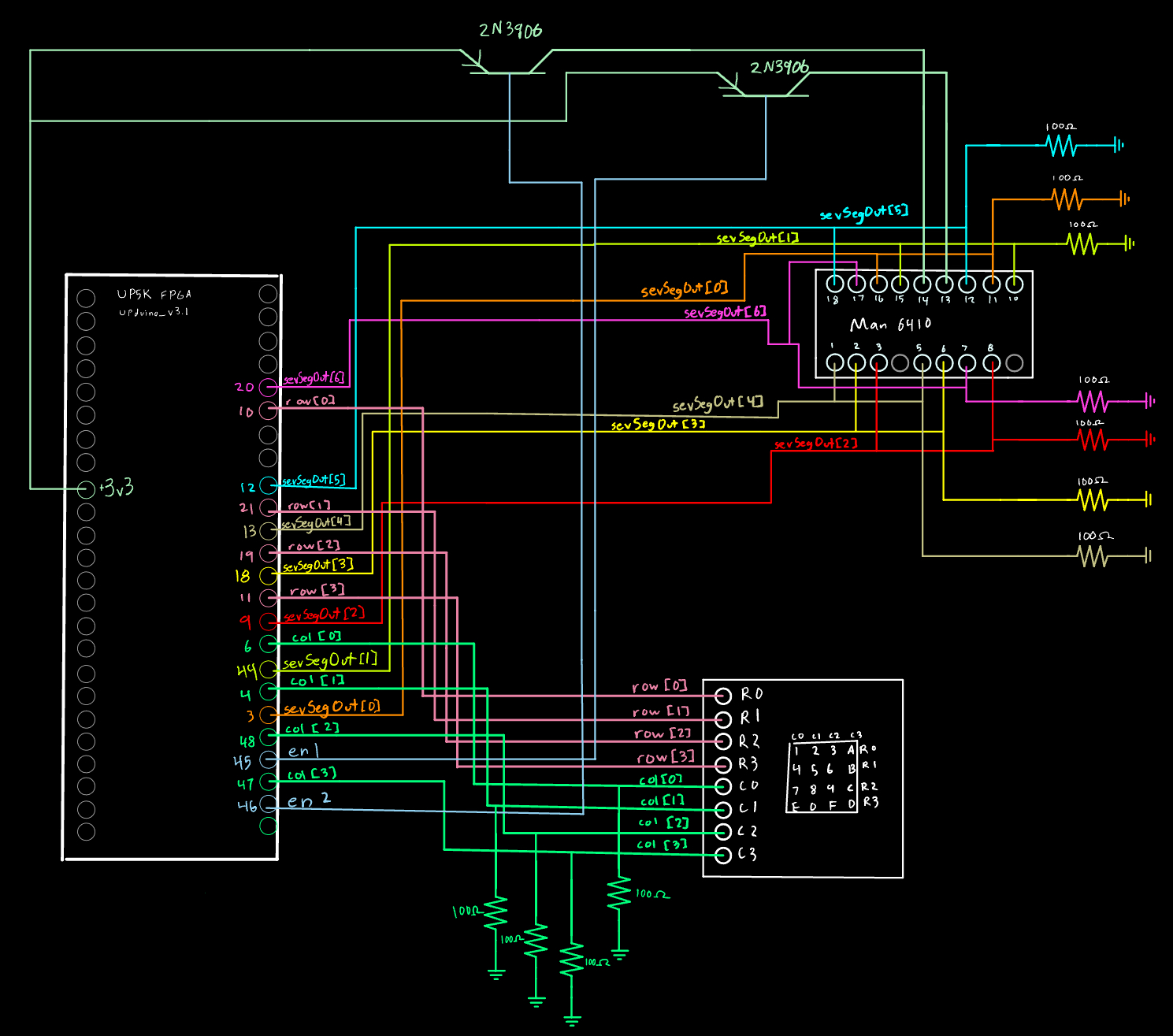
Figure 2 shows the circuit for the design. The LEDs were connected to current limiting resistors of 100 \(\Omega\). These resistor values were solved for by solving for R in V = IR with the voltage found from the part data sheets and a desired current of around 8 mA found from the FPGA data sheet. With voltages of 1.2 and 1.3, 100 \(\Omega\) resistors gave a current slightly above 8 mA. The same calculation was done using 3.3V to find the resistance of the resistors for the transistor base signal. 100 \(\Omega\) resistors were used to pull the column pins to ground.
State Transition Diagram
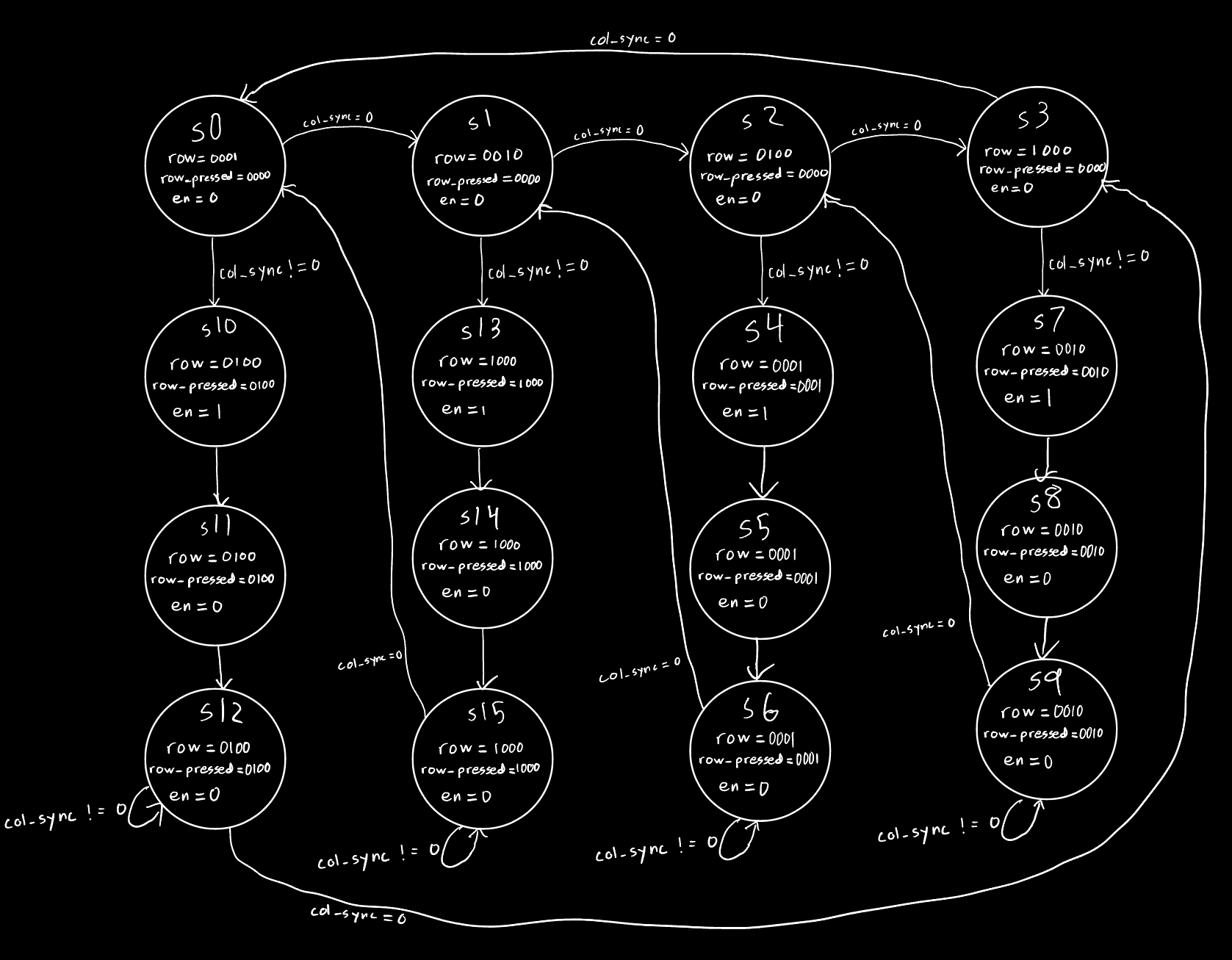
Figure 3 shows the state transition diagam for the design’s FSM. The row checking sections are offset from the row pressed sections due to the synchronizer delaying the column input by two clock cycles. States 4, 5, 7, 8, 10, 11, 13, and 14 are the hold states to deal with switch bouncing.
Next State Logic
| state | col_sync | next |
|---|---|---|
| s0 | 0000 | s1 |
| s0 | !(0000) | s10 |
| s1 | 0000 | s2 |
| s1 | !(0000) | s13 |
| s2 | 0000 | s3 |
| s2 | !(0000) | s4 |
| s3 | 0000 | s0 |
| s3 | !(0000) | s7 |
| s4 | xxxx | s5 |
| s5 | xxxx | s6 |
| s6 | 0000 | s1 |
| s6 | !(0000) | s6 |
| s7 | xxxx | s8 |
| s8 | xxxx | s9 |
| s9 | 0000 | s2 |
| s9 | !(0000) | s9 |
| s10 | xxxx | s11 |
| s11 | xxxx | s12 |
| s12 | 0000 | s3 |
| s12 | !(0000) | s12 |
| s13 | xxxx | s14 |
| s14 | xxxx | s15 |
| s15 | 0000 | s0 |
| s15 | !(0000) | s15 |
Table 1 shows the next state logic for the FSM of the design.
Output Logic
| State | row | row_pressed | en |
|---|---|---|---|
| s0 | 0001 | 0000 | 0 |
| s1 | 0010 | 0000 | 0 |
| s2 | 0100 | 0000 | 0 |
| s3 | 1000 | 0000 | 0 |
| s4 | 0001 | 0001 | 1 |
| s5 | 0001 | 0001 | 0 |
| s6 | 0001 | 0001 | 0 |
| s7 | 0010 | 0010 | 1 |
| s8 | 0010 | 0010 | 0 |
| s9 | 0010 | 0010 | 0 |
| s10 | 0100 | 0100 | 1 |
| s11 | 0100 | 0100 | 0 |
| s12 | 0100 | 0100 | 0 |
| s13 | 1000 | 1000 | 1 |
| s14 | 1000 | 1000 | 0 |
| s15 | 1000 | 1000 | 0 |
Table 2 shows the output logic for the FSM of the design.
Results and Discussion
Testbench Simulation
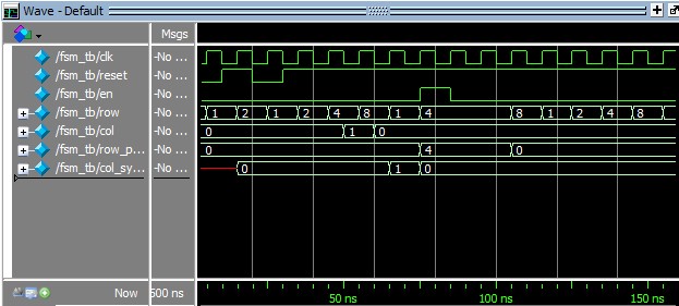
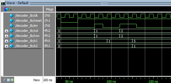
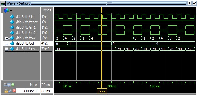
The design met all intended objectives. Figure 4 shows the FSM of the design working in simulation. The rows switch as desired and the module handles an input correctly as seen in the image. Figure 5 shows the FSM decoder working as expected. The waves show the signals switching only when the enable signal is 1. Figure 6 shows the top module working as expected, seen by the correct row outputs and the multiplexed display signal.
Example of Design
In addition to working in simulation, the design also worked in reality. The video above shows an example of the circuit working.
Conclusion
The FPGA was used to read the keypad scanner and display the last two digits pressed. I spent a total of 27 hours on this lab.