Lab 2: Multiplexed 7-Segment Display
Introduction
In this lab, the FPGA was used to drive two seven segment displays using only one set of logic for the display outputs. The FPGA took inputs from two four input DIP switches and displayed the two inputs on two seven segment displays and their sum using seperate LEDs. The main task of this lab was to drive the displays using one seven segment display signal decoder.
Design and Testing Methodology
The task of driving the two displays was done by using a module to multiplex the switch inputs and then feed this signal into the seven segment display decoder module. The on-board high-speed oscillator was used to produce a clock signal, and then the input multiplexer module would then on every positive edge of the clock switch between outputing each switch signal. This output signal was then inputed into a module that decoded the signal into the corresponding signal to drive the LEDs of the display. This LED display signal was one of the outputs of the FPGA in the circuit. Two enable signals were also output for transistors used to drive the displays. The sum of the two inputs was calculated in another module and this sum signal was also outputed by the FPGA. A testbench was created for the adder and input multiplexer modules to test their function in QuestaSim. The seven segment display decoder module is from a previous lab where it was already tested and it is unreasonable to test the oscillator signal in simulation.
The circuit that was made with the FPGA included the two seven segment displays, five LEDs for the sum, and transistors for driving the seven segment displays. The seven segment displays would draw too much current from the FPGA pin, so a transistor was used to help supply current. Two PNP transistors were used, which were switched on and off by the enable signals to drive displaying either digit.
Technical Documentation:
The sourcecode for the project can be found in the Github repository.
Block Diagram
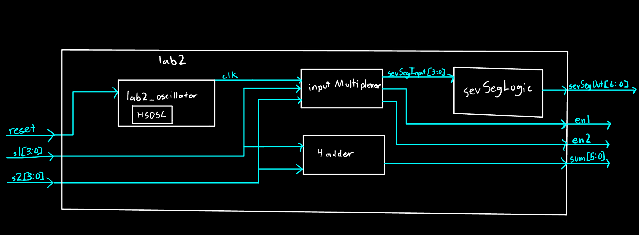
Figure 1 shows the design implimented on the FPGA.
Schematic
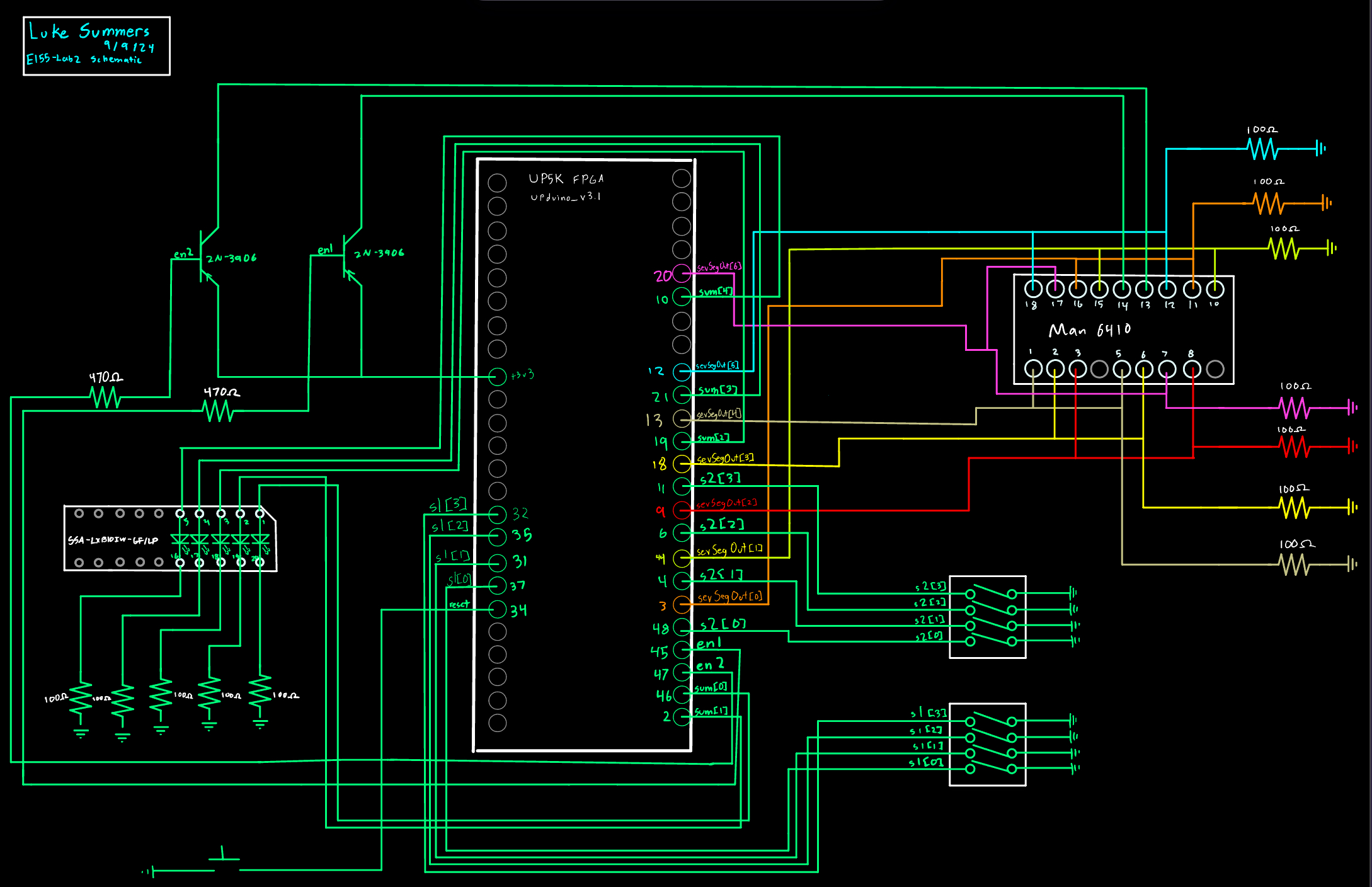
Figure 2 shows the circuit for the design. The LEDs were connected to current limiting resistors of 100 \(\Omega\). These resistor values were solved for by solving for R in V = IR with the voltage found from the part data sheets and a desired current of around 8 mA found from the FPGA data sheet. With voltages of 1.2 and 1.3, 100 \(\Omega\) resistors gave a current slightly above 8 mA. The same calculation was done using 3.3V to find the resistance of the resistors for the transistor base signal.
Results and Discussion
Testbench Simulation
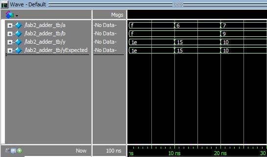
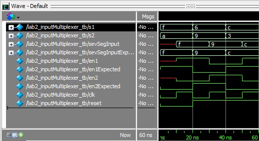
The design met all intended objectives. Figure 3 shows the signals produced by the testbench for the adder module. The expected output is the same as the output, so the adder module was succesful in simulation. Figure 4 shows the signals produced by the testbench for the input multiplexer module. The output signals replicate the expected output signals as the clock cycles, showing this module succesfully multiplexes the signals in simulation.
Example of Seven Segment Displays
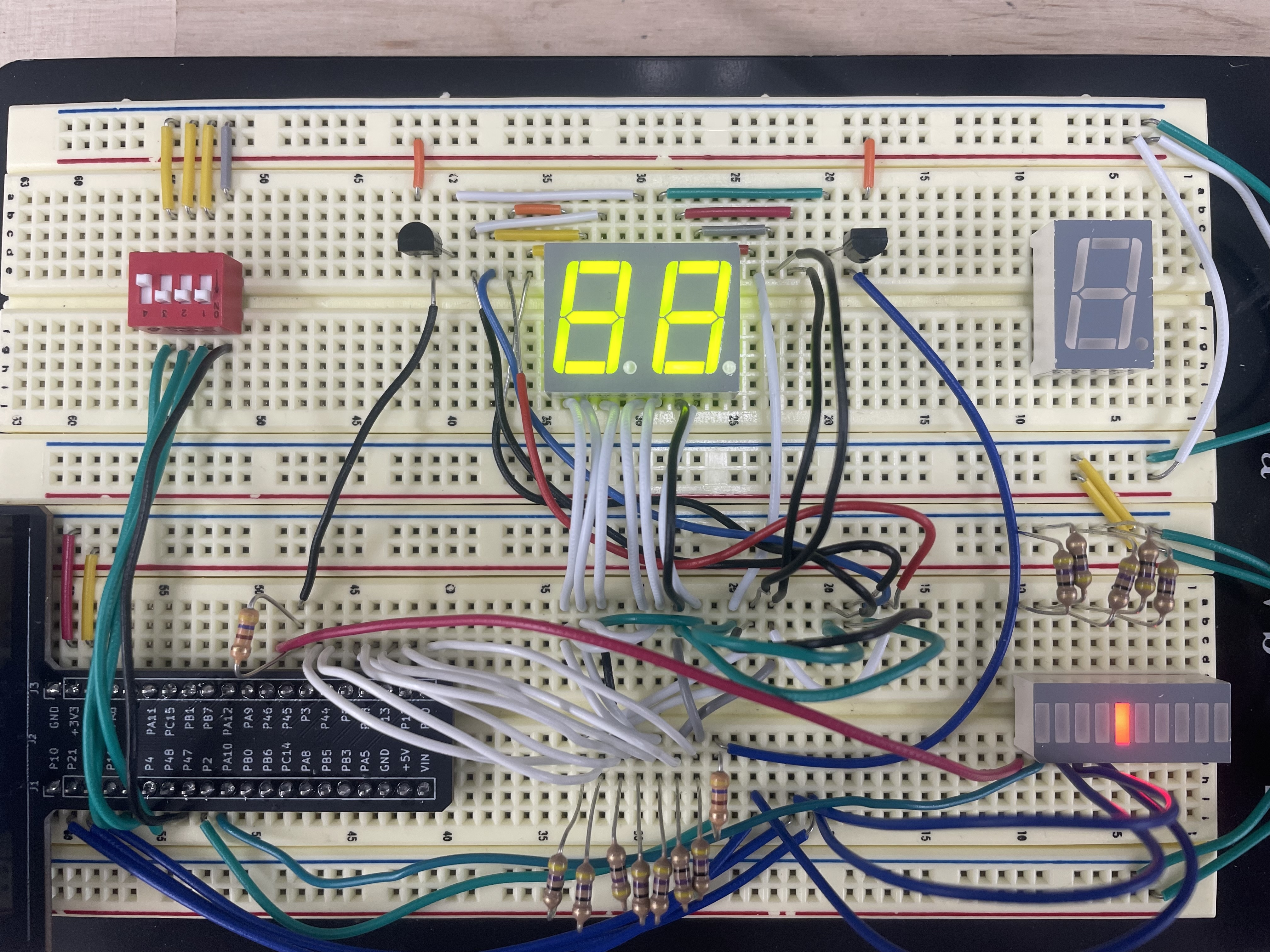
In addition to working in simulation, the design also worked in reality. Figure 5 shows an example of the circuit working. Both switches were inputing ‘1000’, which is 8 as seen on the two seven segment displays. The sum is thus 16 or ‘10000’ which is shown by the fifth LED being lit up on the LED bar in the bottom right of the photo.
Conclusion
The FPGA was used two time multiplex two input signals to drive two seven segment displays in addition to displaying their sum. I spent a total of 12 hours on this lab.