Lab 7: Advanced Encryption Standard Hardware Accelerator
Introduction
In this lab a hardware accelerator for the Advanced Encryption Standard algorithm was designed for a FPGA to carry out 128 bit encryption. An MCU was used to send a key and plain text to the FPGA via SPI for encryption and then confirmed that the encryption was done correctly.
Design
The design consisted of modules that carried out the substition, row permutation, column transformation, and combination with the expanded key. The table for the byte subsitution was loaded into the FPGA’s block RAMs. The subsitution module then could simpily make the subsitution for each byte when necessary. The row permutation module was combinational logic that carried out the required moves. The column transformation module performed a matrix multiplaction on the columns with a fixed matrix. The multiplacation permformed was multiplaction within GF(\(2^8\)). The combination with the expanded key module consisted of an XOR with the portion of the expanded key corresponding to a certian round. For 128 bit encryption, the 4 word key is expanded into a 44 word key. Because the 4 words of the key that correspond to a round only depend on the 4 words of the last round’s key, key expansion could be performed in parrallel to each round of encryption. Before the encryption rounds start, the 4 original key words are XORed with the plaintext, essentially serving as round 0. This means the key expansion module in this round could calculate the words for the next round during this, and this process continued as each subsequent round occurred.
Within the core module for the encryption, the above modules were connected together to create the datapath for the encryption. The core module made use of enabled registers and multiplexers to control the data signals to accurately carry out each round. The module took a load signal as input, and when asserted began the encryption with round 0. In round 0, the key was fed into the key expansion module and the plain text was fed into the key compination module with the key. For rounds 1-9, the key was updated and along with the input to the datapath. On round 10, the column transformation module was skipped in the data path. After round 10 was completed, a output done signal was asserted to signal the the encryption was complete.
The MCU was used to give the FPGA a key and plain text to encrypt via SPI and then recieved the encrypted text back via SPI. The MCU then lit up an LED to signify the encryption was done, and lit up one LED to show that this was succesful or another one if unsuccessful. The top level AES module for the FPGA contained the AES core module and a module to carry out the SPI transactions. When the key and plain text were recieved, the SPI module would assert a load signal to the core module to start the encryption. When the FPGA was done with the encryption, the SPI module would send the encrypted text back to the MCU when the done signal was asserted.
Prior to the design being tested in hardware, it was tested in simulation. Test benches were written and ran for each module within the data path. Then test benches were ran on the core and SPI modules to confirm the encryption and SPI transaction worked as expected in simulation. Once these test benches ran successfully, the design was programmed in hardware and used the LEDs to show the resulting success of the encyrption. A logic analyzer was used to confirm the correctness of the SPI transactions taking place.
Technical Documentation:
The sourcecode for the project can be found in the Github repository.
Schematic
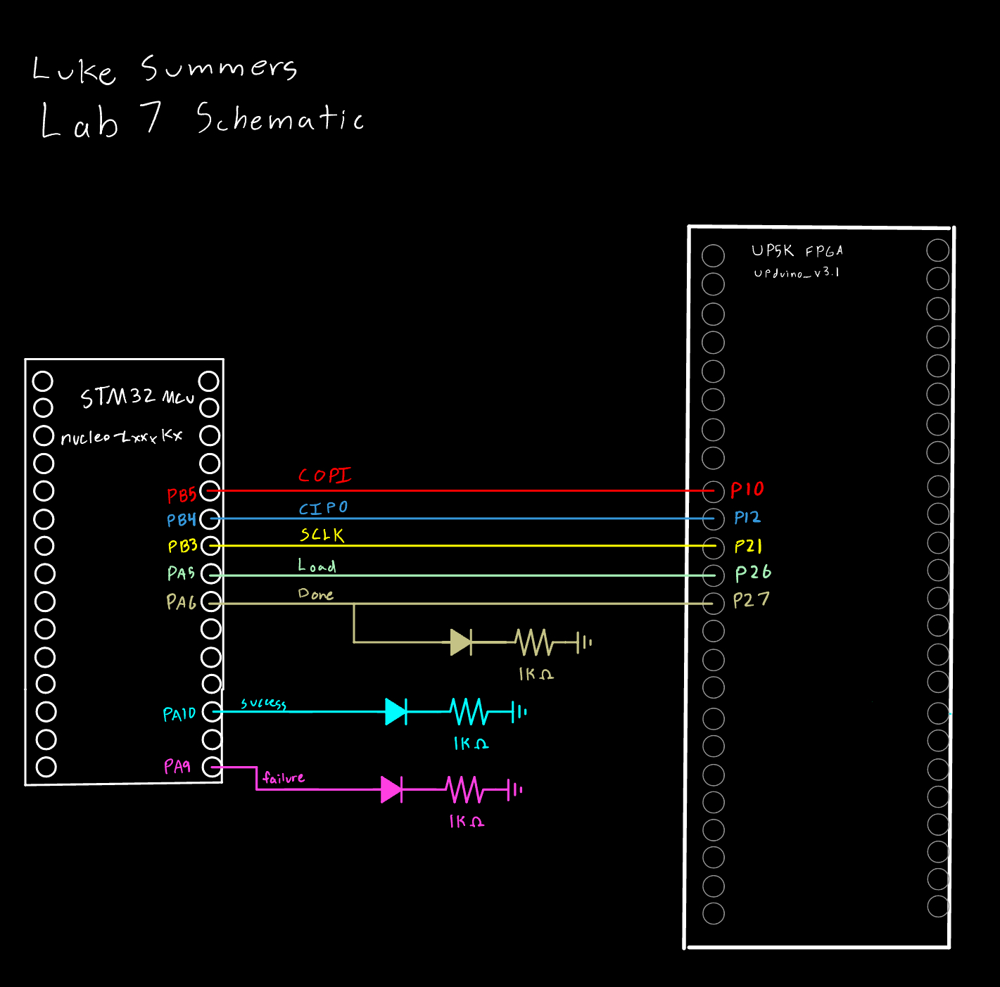
Figure 1 shows the circuit for the design.
Block Diagrams
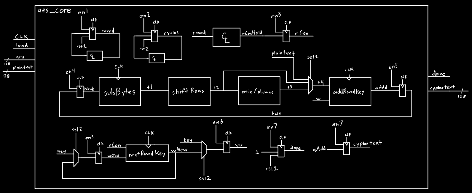
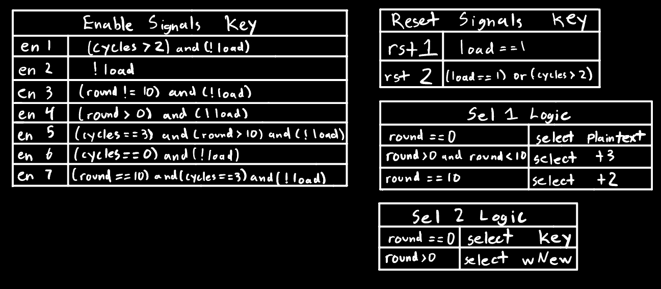
Figure 2 shows the block diagram for the AES core implimented on the FPGA. Figure 3 shows the logic for the enable, reset, and select signals in the core module.
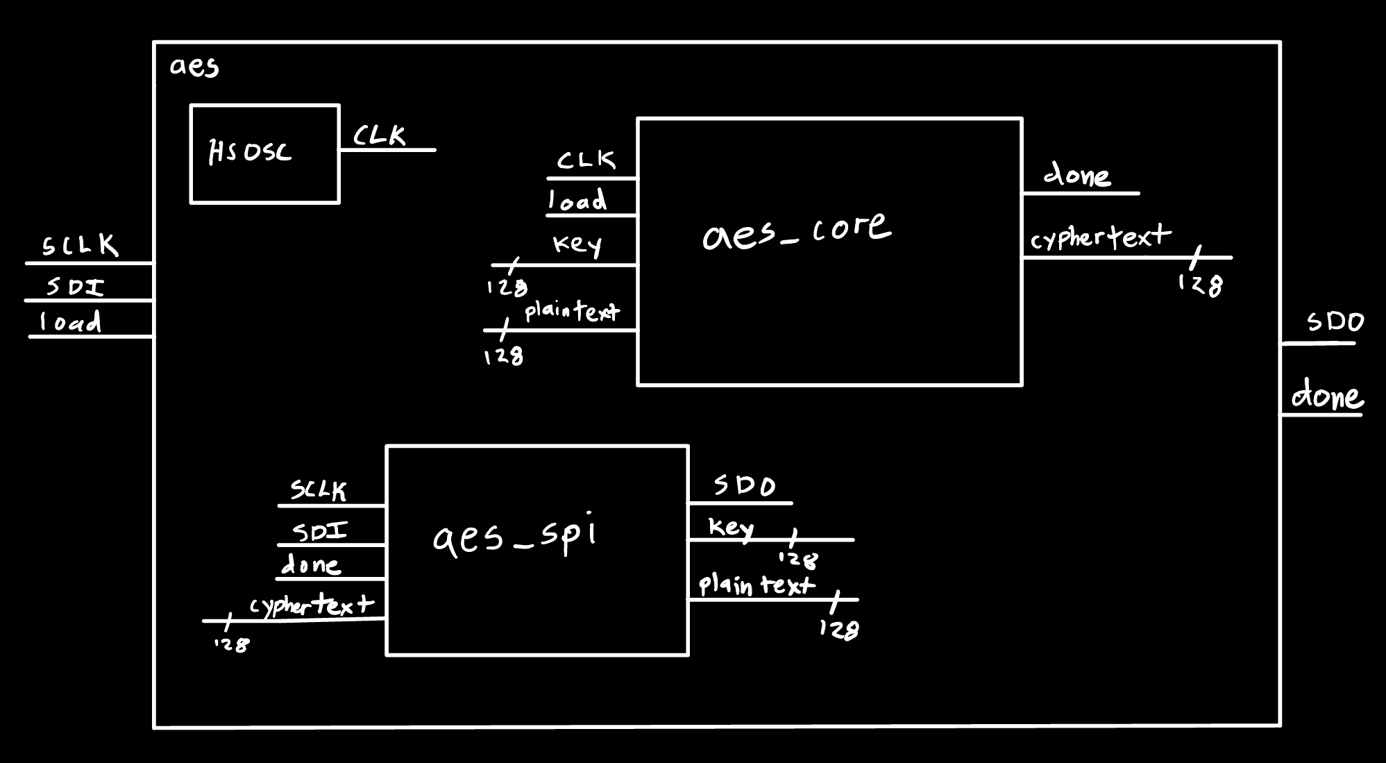
Figure 4 shows the block diagram for the top level AES module implimented on the FPGA.
Results and Discussion
The design was succesful in carrying out encryption according to the AES standard. All modules passed their corresponding test benches in simulation, and the design was able to fit on the FPGA. The FPGA design successfully communicated with the MCU in hardware. Upon a reset to the MCU, which causes it to resend the plain text and key and wait for the cipher text, the light indicating success was lit when the done light was lit. This showed the design worked in hardware.
Example SPI Transaction
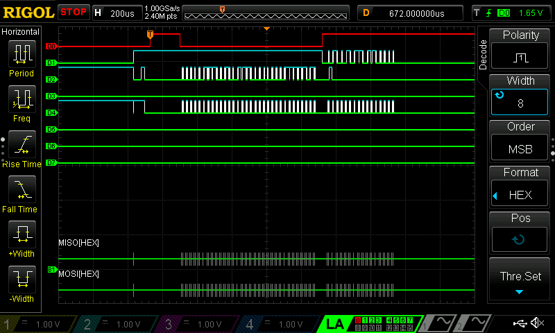
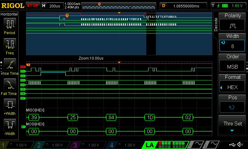
Figure 5 shows an example SPI transaction read on the logic analyzer. Figure 6 shows a zoomed in view of this transaction. The decoded bytes on the CIPO line in the picture show the first 5 words of the cipher text being sent out by the FPGA. These words match the expected values for the first five words.
Conclusion
The design on the FPGA successfully carried out encryption according to the AES standard and successfully communicated with the MCU to carry out an encryption. I spent 12 hours on this lab.